A PCI Dump Switch Card implementation
Sometimes when developing Windows
NT/2000/XP/2003 device drivers the system completely
freezes to the point where only a hardware reset will
resolve the problem. Unfortunately the system state is
completely lost after a hardware reset which makes it
not possible to debug the cause of the system freeze. By
using the PCI Dump Switch Card described in this article
a Windows crash dump file can be saved to disk even if
the system is completely locked up.
Note: we are no
longer selling this card. Most platforms have now
moved to PCI
Express.
By John Gulbrandsen
John.Gulbrandsen@SummitSoftConsulting.com
The PCI Dump Switch Card is a PCI card that induces an NMI
interrupt when the button on the back of the card is pressed. Windows NT 4.0
SP4 and newer platforms (2000, XP, 2003) will create a crash dump file if
special registry settings are enabled. This will allow the state of a frozen
system to be saved into the crash dump and later analyzed in WinDbg (or other
kernel debuggers that understand the NT crash dump file format). Other
operating systems may have similar functionality since the PCI bus is platform
independent but the Dump Switch Card has only been tested on Windows platforms.
Figure 1 below shows the PCI Dump Switch Card and its sub
circuits.
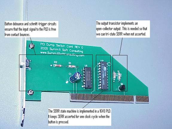
Figure 1.
The three sub circuits of the PCI Dump Switch Card.
The PCI Crash Dump Card asserts the SERR signal on the PCI bus
for one PCI clock cycle when the button is pressed. The SERR signal is then
tri-stated. The SERR signal on the PCI bus is normally routed to the NMI input
on the CPU via the chipset used.
All PCI devices can assert the SERR signal whenever a serious
system error has occurred. On most motherboards the SERR signal is used to
detect memory parity errors. Because of this a 'parity error' message may be
displayed by Windows NT when the button is pressed on the Dump Switch Card (the
exact message is dependant on the system hardware or rather by the HAL used for
the target hardware).
The SERR signal is a wire-or signal that is common for all PCI
devices. The PCI bus has a pull-up resistor on the SERR signal so the PCI
devices should only pull SERR down when a device wants to assert SERR, they
never drive SERR. The output transistor stage on the PCI Dump Switch Card
implements an open collector output which pulls down SERR when the output from
the PLD is asserted.
Note that in rare cases, some PC's do not map the SERR signal
to the NMI of the CPU. On these platforms it is not possible to create a Crash
Dump using dump switch cards like the one described in this article.
In this section each of the sub circuits will be explained in
detail. As figure 1 above and figure 2 below show the main sub circuits are the
debounce and Schmitt-trigger, the PLD implementation of the SERR state machine
and the open collector output switch circuits.
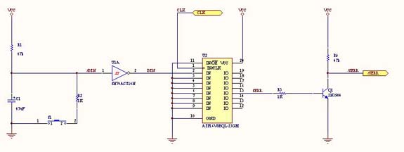
Figure
2. The circuit diagram for the Dump Switch Card.
The BTN signal fed to the PLD must be clean and free from
contact bounces or else the state machine will not work correctly. This is
accomplished by using a simple RC circuit and a Schmitt trigger inverter as
shown below in figure 3.
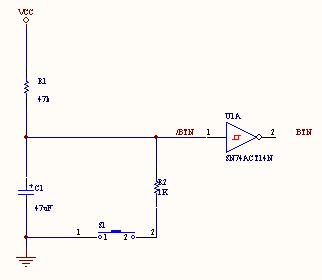
Figure 3. The button
debounce and Schmitt trigger circuit.
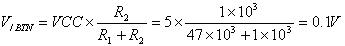
Normally, when the switch is open, the capacitor C1 is charged
via R1 to VCC. When the button S1 is pressed down (is closed) the capacitor C1
is discharged through R2 to ground. R1 and R2 are chosen so that the voltage
divider output /BTN is a valid logic low when S1 is closed:
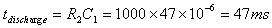
 ; which is firmly
in the TTL logic low range. ; which is firmly
in the TTL logic low range.
The time constant of the R2C1 RC-circuit is chosen so that the
discharge time is a few times greater than the contact bounces of the switch
used. Since the switch used has contact bounces approximately 5ms we have
chosen a C1 discharge time 10 times higher which will ensure that the
Schmitt-trigger inverter U1 will toggle its output state when the button S1 no
longer bounces:
Note that the Schmitt-trigger inverter will toggle its output
before C1 is fully discharged and charged because its thresholds for going
positive and negative is around 1.5 and 1.0 volts respectively. Figure 4 below
shows that in reality the Schmitt-trigger toggles 80 ms after the button has
been pressed.
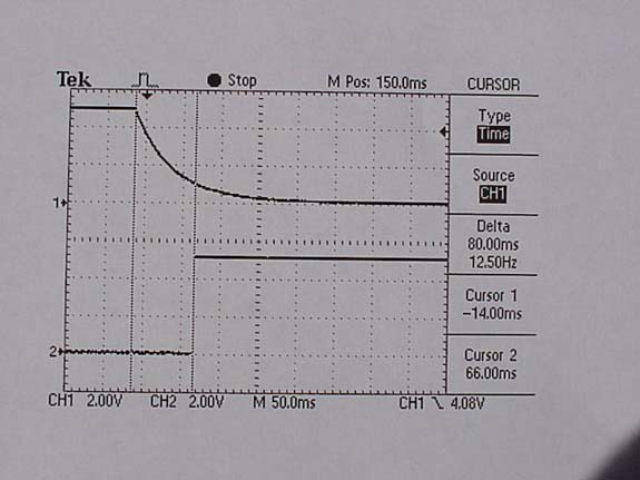
Figure
4. Oscilloscope image of the /BTN and BTN signals.
After a discharge (when the button is released) it takes
approximately
 to
recharge the capacitor. to
recharge the capacitor.
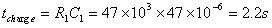
Like previously explained the Dump Switch Card must assert
SERR during one PCI clock cycle and then tri-state SERR. In order to ensure
this timing requirement as described in the PCI specification we needed to
implement the state machine shown below in figure 5:
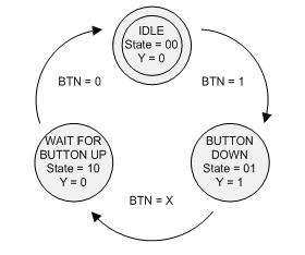
Figure
5. The SERR state machine.
The state machine starts in the IDLE state (00) and stays
there as long as the button is not pressed (as long as the BTN input to the PLD
is 0). As soon as the button is pressed (BTN = 1) a transition to the next
state (01) is made. The output is also changed from 0 to 1 when in state 01
(because the output is associated with the states and not with the transitions
this is a Moore-type state machine). The state machine stays in state 01 until
the next clock cycle when a transition to state 10 is made. The output is
changed back to 0 which was the requirement per the PCI specification for the
SERR signal. Note that the state of the button is don't care for the transition
to state 10 to occur since we are only interested in staying in state 01 for
one clock cycle.
Note that we must wait in state 10 until the button has been
released (BTN = 0) because the state machine would otherwise run a second
sequence through the state machine. In other words, the state machine will
produce a '1' on the output for exactly one clock cycle regardless how long the
button is pressed.
Since we were to implement the state machine in a simple 16V8
PLD we choose to work with a low-level abstraction of the state machine. We
therefore directly derived the next-state Boolean functions by using
Karnaugh-maps, created a WinCUPL source file and finally programmed the PLD
using a PLD programmer. Because of the simple nature of the 16V8 PLD we cannot
use a higher-level HDL like Verilog or VHDL. Figure 6 below shows the
next-state table directly derived from the state machine in figure 5.
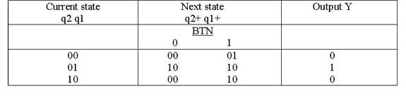
Figure
5. The next-state table for the SERR state machine.
We then used the Karnaugh maps shown below in figure 6 to
derive the Boolean functions for the next state.
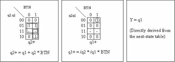
Figure 6.
The next-state Boolean functions are derived using Karnaugh maps.
The next-state Boolean equations can now be used to implement
the next-state logic using either discrete gate logic shown below in figure 7
or be programmed into a PLD. We decided to use a PLD since this reduces the
number of circuits on the board and it also gives us an easy way to modify the
next-state logic in case we need to make adjustments to the state machine.
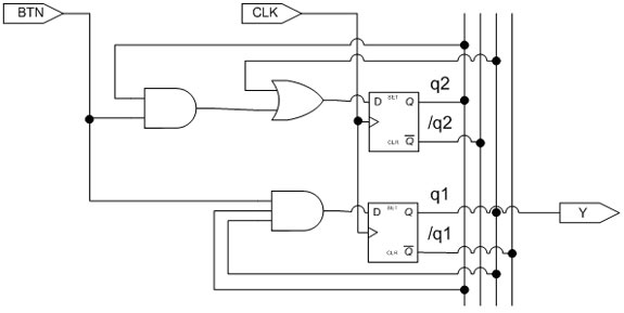
Figure 7.
Example of an implementation of the SERR state machine using discrete gates.
Our PLD logic was implemented using WinCupl. Figure 8 below
shows the WinCUPL source code for the SERR state machine.
Name DumpSwitch ;
PartNo 00 ;
Date 5/22/2005 ;
Revision 01 ;
Designer John Gulbrandsen ;
Company Summit Soft, Inc. ;
Assembly None ;
Location ;
Device g16v8 ;
/* *************** INPUT PINS *********************/
PIN 2 = BTN; /* Input */
PIN 1 = CLK;
/* *************** OUTPUT PINS *********************/
PIN 13 = Q2; /* State variable */
PIN 14 = Q1; /* State variable */
PIN 15 =
Y; /* Output */
/* *************** NEXT STATE EQUATIONS *********************/
Q2.D =
Q1 # Q2 & BTN;
Q1.D = !Q2 & !Q1 & BTN;
/* *************** OUTPUT EQUATIONS *********************/
Y =
Q1;
Figure 8.
The WinCUPL source code for the SERR state machine implementation in a 16V8
PLD.
As the WinCUPL source code in figure 8 above shows we have
chosen to use pin 2 as the BTN input, pin 1 as CLK input and pin 15 as Y
output. The schematic for the PLD is shown below in figure 9.
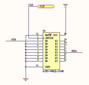
Figure
9. The input and output connections on the PLD.
Before programming the PLD the state machine was simulated
using WinSIM which comes with the WinCUPL distribution from Atmel. Figure 10
below shows the behavior of the SERR state machine. As can be seen Y goes high
for one clock cycle when BTN goes high (Y clock 4). The state machine waits
until BTN = 0 before going back to the idle state (Q2 clock 8). Two full cycles
are simulated (the second cycle which starts in clock 14 is identical to the
first cycle - this proves that the state machine is correctly reset after the
first sequence.
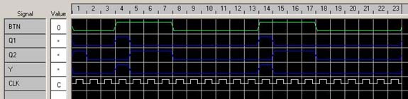
Figure 10.
Simulation of the SERR state machine in WinSim.
Once simulated, the PLD was programmed using a regular PLD programmer.
We need to create a tri-state circuit outside the PLD since the PLD used (Atmel
ATF16V8B) doesn't support tri-stating its outputs via software. We chose to use
a simple switch transistor (2N3904) in open-collector configuration. The
open-collector output circuit is shown below in figure 11.
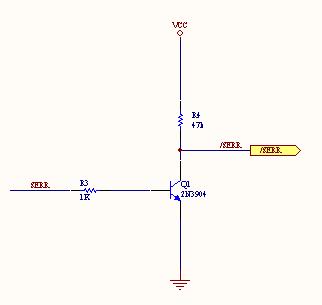
Figure 11.
The tri-state output is implemented with an NPN transistor in open-collector
configuration.
The resistor R4 in figure 11 above is used to test the Dump Switch Card on the
bench in a laboratory environment. The PCI bus normally uses a 2K resistor as
pull-up resistor on the /SERR signal. Since 47K is very large in relation to 2K
the parallel resistance between 47K and 2K is close to 2K. Therefore the R4 was
left populated in the production series of the dump switch card.
To enable the NMI crash dump support in Windows NT 4.0 SP4 and newer versions
(Windows 2000, XP and 2003) create the NMICrashDump DWORD value in the
HKEY_LOCAL_MACHINE \ SYSTEM \ CurrentControlSet \ Control \ CrashControl branch
in the registry. Set the value to 1 to enable the Dump Switch Card and 0 to
disable the crash dump feature. Also enable writing the dump file in the
'system' control panel applet. Note that you have to reboot the system for the
change to take effect.
Download the .reg files that enable and disable the crash
dump support here:
NmiCrashDump.zip
Figure 12 below shows what the screen should look like when the dump switch
feature has correctly been activated by the Dump Switch Card.
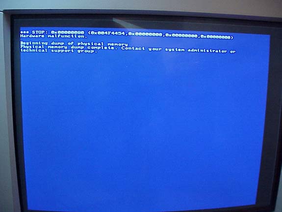
Figure
12. A completed dump induced by the PCI Crash Dump Card.
If the NMICrashDump value is missing from the registry Windows NT / 2000 / XP /
2003 thinks that a hardware error has occurred and the screen shown below in
figure 13 is displayed.
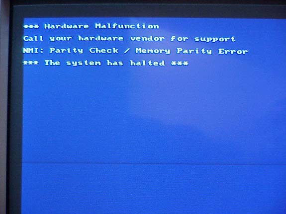
Figure 13.
The screen showed when the Dump Switch Card is activated without the
NMICrashDump registry value being present.
Further Reading
1) The basis for the Dump Switch
Card is the following article by Microsoft:
Dump
Switch Support for Windows.
2) The PCI Specification (any
version) describes the SERR functionality. The PCI specification can be be
ordered from http://www.pcisig.com/specifications.
About the Author
John Gulbrandsen is the founder
and president of Summit Soft Consulting. John has a formal background in
Microprocessor-, digital- and analog- electronics design as well as in embedded
and Windows systems development. John has programmed Windows since 1992
(Windows 3.0). He is as comfortable with programming Windows applications and
web systems in C++, C# and VB as he is writing and debugging Windows kernel
mode device drivers in SoftIce.
To contact John drop him an email:
John.Gulbrandsen@SummitSoftConsulting.com
About
Summit
Soft Consulting
Summit Soft Consulting is a
Southern California-based consulting firm specializing in Microsoft's operating
systems and core technologies. Our specialty is Windows Systems Development
including kernel mode and NT internals programming.
To visit Summit Soft Consulting on
the web: http://www.summitsoftconsulting.com

|