A Microchip PIC-Compatible RISC CPU IP Core
This article describes the hardware
design and Verilog implementation of a RISC CPU IP
core compatible with the Microchip PIC10F200-series of
microcontrollers. The CPU IP Core was designed for a
client where a small but very fast CPU needed to be
implemented in an FPGA. Since the code is running from
on-chip RAM cells, the speed of the CPU IP Core is
around 50 times faster than the original Microchip
PIC10F200-series
implementation.
Note that this article is a short
summary of the design and implementation of the RISC CPU
IP Core. The detailed design documentation can
be downloaded here
in PDF format. Full Verilog source code including a
complete set of test benches is available here.
By John Gulbrandsen
John.Gulbrandsen@SummitSoftConsulting.com
The PIC10 IP Core is an instruction-compatible Verilog
implementation of the Microchip PIC10F200-series microcontrollers. We chose to
implement the PIC10F200-series CPU because of the small but effective RISC CPU
architecture and the availability of free software development tools from
Microchip. The PIC10F200-series of microcontrollers only has 33 instructions
which makes the final hardware implementation compact. The CPU can address up
to 512 instruction words which is small enough to fit on-chip but still large
enough to be practically useful when programmed in assembly language. Figure 1
below shows the main modules of the PIC10 RISC CPU IP Core.
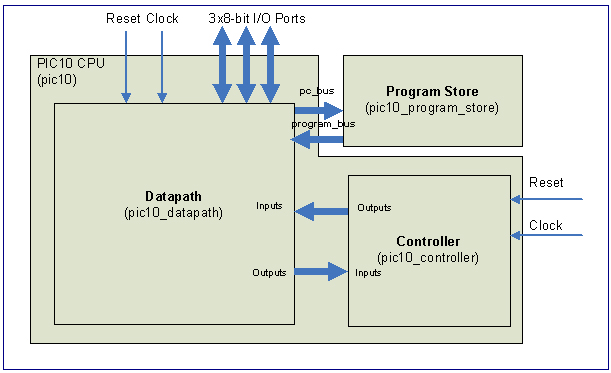
Figure 1.
The main modules and interconnects in the PIC10 RISC CPU IP Core.
As figure 1 shows, the pic10 module contains the
pic10_datapath and pic10_controller modules while the pic10_program_store
is external to the CPU Core. This means that the Program Store can be located
off-chip if needed. Locating the Program Store on-chip however enables the CPU
Core to execute at the internal clock speed of the FPGA which results in very
fast clock frequency compared to the original PIC10F200.
Datapath Architecture
Figure 2 below shows a somewhat
simplified datapath architecture where the eight Special Function Registers
0..7 are not shown. This datapath is sufficient to execute most instructions so
it will be used to introduce the overall PIC10 CPU IP Core architecture.
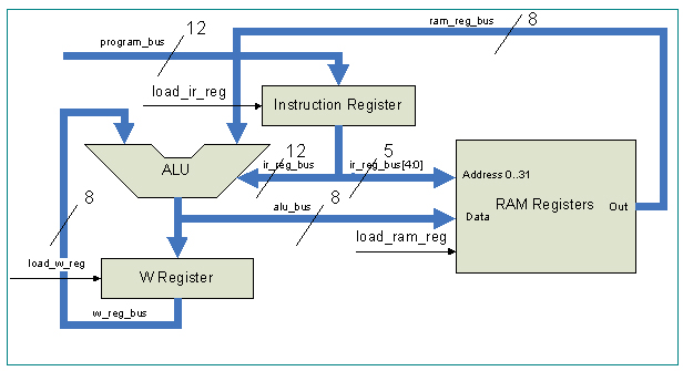
Figure 2. A simplified datapath that
illustrates the basic datapath architecture.
Most instructions in the PIC10F200 architecture operate on
either the 'W' or one of the 'f' registers. The 'W' register is input as the
ALUs first operand while the currently addressed 'f' register is input as the
second ALU operand. The ALU result is output on 'alu_bus' from where it is
loaded into either the 'W' register or into the currently addressed 'f'
register. The Controller either asserts the 'load_w_reg' or the 'load_ram_reg'
depending on if the instruction word in the instruction Register directs the
result to the 'W' or 'f' register respectively.
In order for the ALU to be able to update the STATUS register
bits Z, C, and DC a separate 'status_bus' exists together with three control
signals named 'load_z', 'load_d' and 'load_dc'. These signals are displayed
below in figure 3. Also note that figure 3 contains the 'ALU Mux' on operand
input two which allows the Controller to select the second ALU operand to come
from either the RAM Registers (shown above in figure 2) or from one of the
eight SFR Registers 0..7.
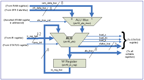
Figure 3. The actual datapath surrounding the ALU.
The ALU knows from the 'ir_reg_bus' which instruction word is currently
being executed. The 'carry_bit' input is connected to the C bit in the STATUS
register. This is used during additions and subtractions. The 'ram_data_bus'
input to the ALU Mux comes from the RAM registers as shown above in figure 1.
The 'sfr_data_bus' comes from the currently addressed SFR register.
The PIC10 architecture allows both direct and indirect addresses. A direct
address is encoded directly in the 12-bit instruction word while an indirect
address is taken from the FSR Special Function Register. The address generation
logic is shown below in figure 4.
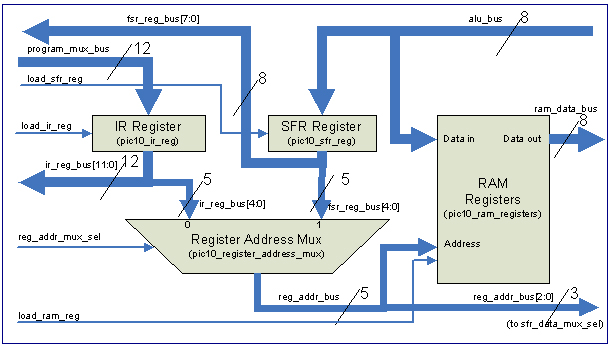
Figure 4. The Register Address Mux selects either a direct or
indirect address.
As can be seen in Figure 4, the Register Address Multiplexer passes through
either the 'fffff' field in the instruction word (bits 4:0) or the value in the
SFR register. The 'reg_addr_mux_sel' signal determines which source bus to
route to 'reg_addr_bus'.
The PIC10 CPU architecture has a two-level stack that enables subroutines to be
called via the CALL/RETLW instruction pair. Jumps to an absolute address can
also be done via the GOTO instruction. Figure 5 below shows the Program Counter
Datapath required to allow the CALL, RETLW and GOTO instructions to be
implemented.
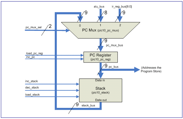
Figure 5. The Program Counter Datapath allows the PC to pushed,
popped and loaded from 'alu_bus'.
As Figure 5 shows, the 'pc_mux_sel' input selects the source of the data on
the 'pc_mux_bus'. The 'pic10_pc_reg' register is loaded on the rising edge of
the clock signal when the 'load_pc_reg' signal is asserted. The 'inc_pc' signal
is used to increment the Program Counter as each instruction is executed. The
'inc_stack' and 'dec_stack' signals are used to select which stack register
will be loaded when the 'load_stack' signal is asserted. The 'stack_bus' always
outputs the data in the current stack location (i.e. the data previously
written to the stack location).
The PIC10 CPU IP Core contains three bidirectional 8-bit I/O ports while the
Microchip PIC10F20x architecture only has a single GPIO register (where only 4
bits are implemented due to lack of pins on the package). The I/O port bits can
individually be programmed as input or output via the TRIS instruction. The
output data (for output ports) is programmed into GPIO registers 5, 6 and 7
(where GPIO registers 5 and 7 replaces the not implemented OSCCAL and CMCON0
registers). Figure 6 below shows the internal architecture of the
'pic10_tri_state_port' module.
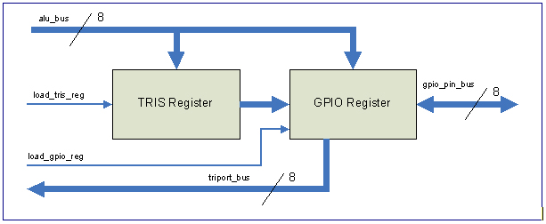
Figure 6. The 'pic10_tri_state_port' module contains the 8-bit
bi-directional I/O port logic.
As can be seen in figure 6, the 'alu_bus' input allows the TRIS and
GPIO 8-bit registers to be loaded from 'alu_bus. A TRIS registers (5, 6 or 7)
is loaded from 'alu_bus' when a TRIS instruction is executed. A GPIO register
(5, 6 or 7) is loaded when Special Function Registers 5, 6 or 7 is the write
target of an instruction (i.e. MOVWF).
Controller Architecture
As shown in Figure 1, the 'pic10_controller' module is connected via
a number of inputs and outputs to the 'pic10_datapath' module. The controller
is responsible for decoding the current instruction in the IR register and set
up the datapath control signals so that the data is correctly routed from the
source to the destination register accordingly to the semantics of the
instruction. As the instruction in the IR changes so does the functionality of
the Controller. The Controller is essentially a simple state machine that
asserts a pre-determined number of signals for the various instructions. Figure
7 below shows the inputs and outputs of the 'pic10_controller' module.
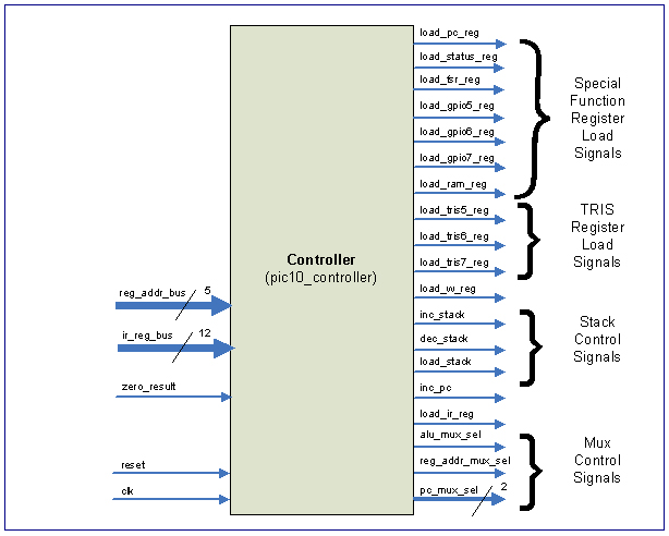
Figure 7. The input and output signals on the
Controller module.
For detailed information of the control signals that get asserted
for each of the 33 instructions in the PIC10 instruction set please see the
full documentation (PDF format). The full documentation contains sections that
describe the datapath control signals that need to be asserted for each
instruction. The path the data is routed from the source to the destination
register are illustrated via block diagrams as well as via pseudo Verilog code.
Please refer to the Microchip PIC10F200/202/204/206 data sheet for the detailed
syntax and description of the various instructions.
Source Code
The Verilog source code for the
PIC10 RISC CPU IP Core can be downloaded
here. The zip file also contains test benches for all of the modules.
Further Reading
1) The Microchip
PIC10F200/202/204/206 Data Sheet is available on
Microchip's web site.
2) For a very good introduction
and reference to the Verilog HDL be sure to read "Verilog HDL" by Samir
Palnitkar. ISBN 0-13-044911-3
3) For advanced HDL design and
implementation, "Advanced Digital Design with the Verilog HDL" by Michael D.
Cilette is recommended. ISBN 0-13-089161-4.
About the Author
John Gulbrandsen is the founder
and president of Summit Soft Consulting. John has a formal background in
Microprocessor-, digital- and analog- electronics design as well as in embedded
and Windows systems development. John has programmed Windows since 1992
(Windows 3.0). He is as comfortable with programming Windows applications and
web systems in C++, C# and VB as he is writing and debugging Windows kernel
mode device drivers in SoftIce.
To contact John drop him an email:
John.Gulbrandsen@SummitSoftConsulting.com
About
Summit
Soft Consulting
Summit Soft Consulting is a
Southern California-based consulting firm specializing in Microsoft's operating
systems and core technologies. Our specialty is Windows Systems Development
including kernel mode and NT internals programming.
To visit Summit Soft Consulting on
the web: http://www.summitsoftconsulting.com

|